SerDes
Testing and analysis of a SerDes prototype chip
Overview
This project involves the testing and analysis of a SerDes prototype chip based on the 180 nm CMOS process. The primary focus is to evaluate the chip’s performance under different configurations and ensure optimal functionality.

SerDes Structure
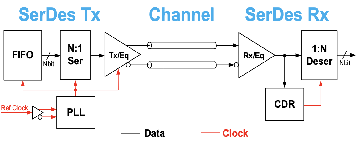
- Transmitter (Tx):
- Encoder, PLL, Serializer
- Receiver (Rx):
- Clock Data Recovery (CDR), Deserializer, Decoder
- Equalizer:
- Ensures signal integrity
- Clock Data Recovery (CDR):
- Recovers clock from data flow
Methodology
- Configure and verify the normal operation of the chip.
- Adjust changeable parameters to achieve the best performance.
- Send Pseudo-Random Binary Sequence (PRBS) codes.
- Measure relevant performance metrics using test platforms and analysis tools.
Test Platform Components:
- Logic Control: Configure via serial machine codes.
- DAC: Controls voltage of the VCO for CDR functionality.
- ASIC Equalizer Configuration: Adjust signal integrity parameters.
- AD9522 PLL: Configures the reference clock.
- PRBS Code Generator: Built-in generator to send parallel pseudo-random codes.
Software Analysis:
Analyze the resulting data, including error rates and signal quality.
Results
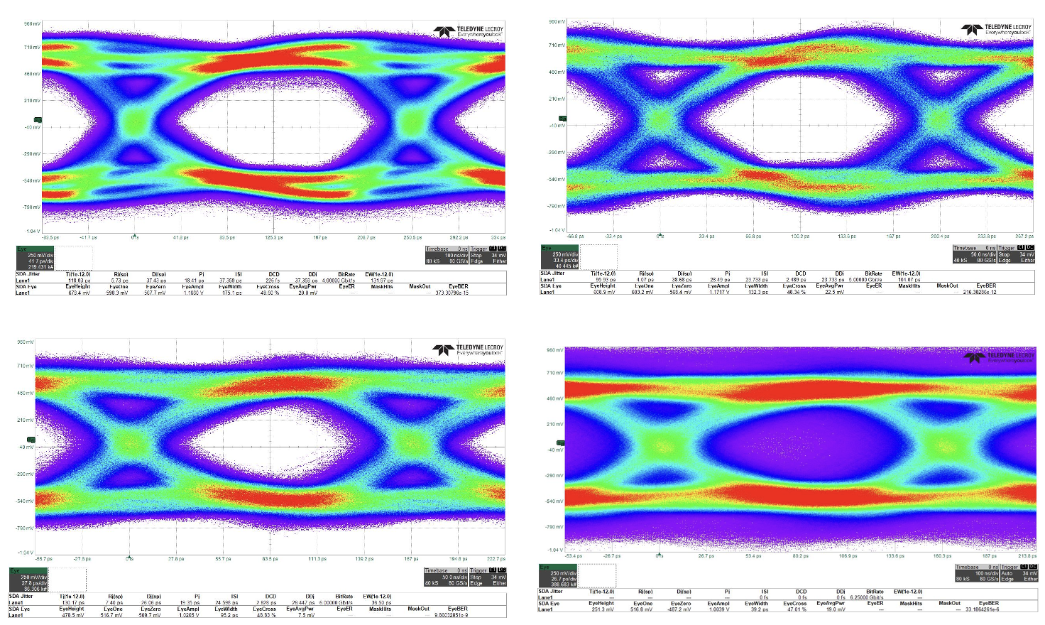
Eye Diagram Analysis:
- Evaluates signal quality.
- Reflects interference and jitter.
- Helps determine the optimal sampling time.
Images and Captions


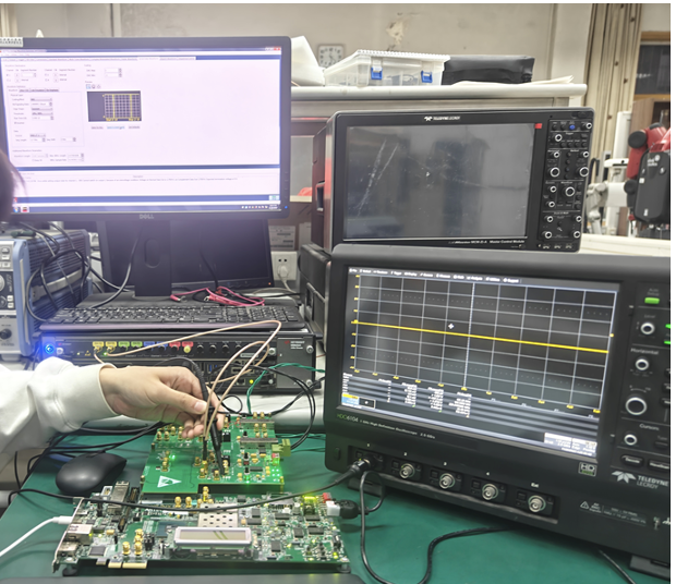
Left: Test platform setup showcasing equipment and connections. Right: Measured eye diagram highlighting signal quality and interference.
Takeaway
The test results provide insights into the signal quality and overall performance of the SerDes chip. The findings help improve the prototype for future iterations and refine the design for better efficiency and signal integrity.